Engineer 'builds a GPU from scratch' in two weeks
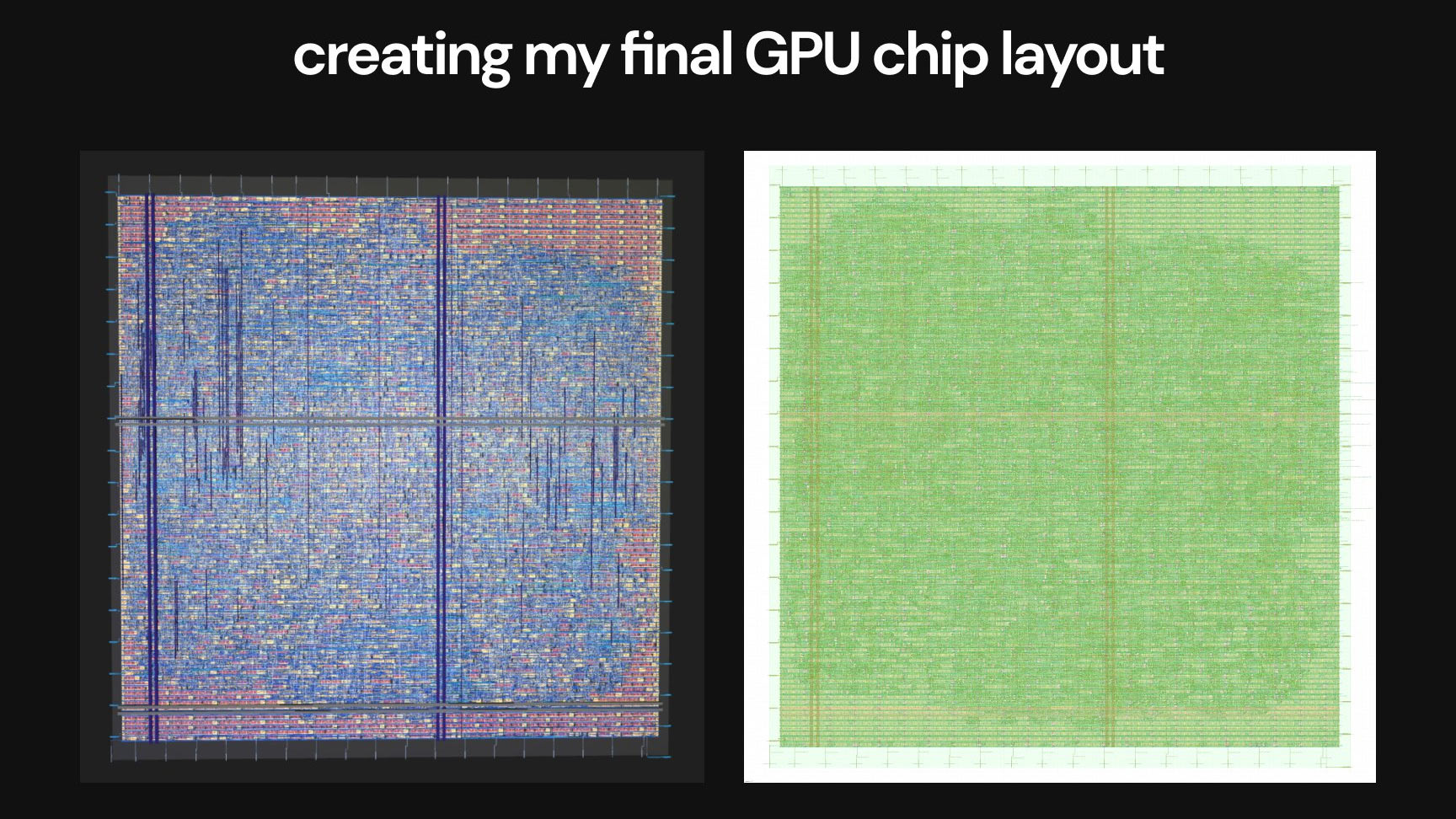
An engineer has shared his journey in “building a GPU from scratch with no prior experience.” As with his prior project of designing a CPU from scratch, Adam Majmudar took just two weeks to complete this cerebral feat. In a Twitter/X thread Majmudar takes us through the process, step-by-step, and admits GPU designing was a much harder task than expected. To be clear, the current conclusion of the project is a chip layout in Verilog which was finally passed through OpenLane EDA software to verify it. However, the GPU is going to be submitted for tapeout via Tiny Tapeout 7 so is destined to become a physical chip in the coming months.
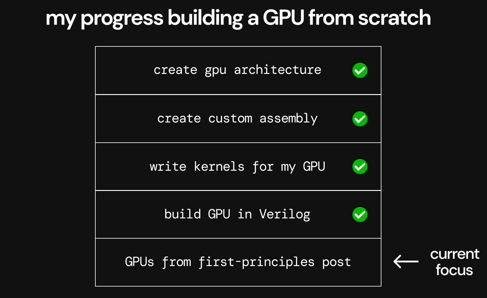
Above you can see the flow of tasks Majmudar worked through to design his GPU. Yet, as a ‘from scratch’ project, a lot of study and thought was required even before the first step was tentatively taken. Last time we highlighted the engineer’s concerns that GPUs would be a relatively difficult field of study, due to the dominance of proprietary tech, as that prediction came true.
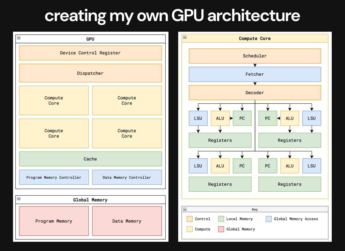
Through several iterations of the above architecture, Majmudar decided to focus on general-purpose parallel computing (GPGPUs) capabilities. Thus he adjusted his Instruction Set Architecture (ISA), which features just 11 instructions, to achieve this goal. Next up, the engineer wrote two matrix math kernels to run on his GPU. These matrix addition and multiplication kernels would demonstrate the key functionality of the GPU and provide evidence of its useful application in graphics and machine learning tasks.
Article continues below
It had been relatively easy for the engineer so far, but building his GPU in Verilog presented “many issues.” Advice from the (in)famous George Hotz helped Majmudar move past one of his first (and second) hurdles regarding memory and a warp-scheduler implementation. A third rewrite of his code did the trick though, fixing compute core execution scheduling.
Some more unspecified redesigns later and the proof of the pudding, a video showing the matrix addition kernel running and validating, was shared in the Tweet thread.
Lastly, the completed Verilog design was passed through OpenLane EDA, targeting the Skywater 130nm process node (for Tiny Tapeout). Again some issues needed to be ironed out. In particular, Majmudar explains that some Design Rule Checks (DRCs) failed and necessitated rework.
After the two-week effort, the engineer enjoyed playing with a cool 3D visualization of his GPU design. That will have to suffice until TT7 returns silicon to participants. Of course, the work isn't going to rank among the best graphics cards. If you want to read more about this homemade GPU check out the entertaining social media thread and / or investigate the dedicated Tiny-GPU GitHub page.
Get Tom's Hardware's best news and in-depth reviews, straight to your inbox.


